Intel Builds the World’s Largest Neuromorphic System
Intel has built the world's largest neuromorphic system code-named Hala Point.
Samsung Electronics announced that its Foundry Business has commenced mass production of System-on-Chip (SoC) products built on its second generation 10-nanometer (nm) FinFET process technology, 10LPP (Low Power Plus).
10LPP process technology allows up to 10-percent higher performance or 15-percent lower power consumption compared to its first generation 10nm process technology, 10LPE (Low Power Early). As this process is derived from the already proven 10LPE technology, it offers advantages by greatly reducing turn-around time from development to mass production and by providing significantly higher initial manufacturing yield. SoCs designed with 10LPP process technology will be used in digital devices scheduled to launch early next year.
“We will be able to better serve our customers through the migration from 10LPE to 10LPP with improved performance and higher initial yield,“ said Ryan Lee, vice president of Foundry Marketing at Samsung Electronics. “Samsung with its long-living 10nm process strategy will continue to work on the evolution of 10nm technology down to 8LPP to offer customers distinct competitive advantages for a wide range of applications.“
Samsung also announced that its newest manufacturing line, S3, located in Hwaseong, Korea, is ready to ramp up production of process technologies including 10nm and below. S3 is the third fab of Samsung’s Foundry Business, following S1 in Giheung, Korea and S2 in Austin, USA. 7nm FinFET process technology with EUV (Extreme Ultra Violet) will also be mass produced at S3.
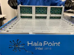
Intel has built the world's largest neuromorphic system code-named Hala Point.

Meta Platforms unveiled the second generation of its Meta Training and Inference Accelerator (MTIA) AI chip.

Intel announced its latest chip to challenge Nvidia’s dominant market position for semiconductors that train and deploy large AI models.


