AMD Achieves First TSMC N2 Product Silicon Milestone
AMD announced that its next-generation EPYC processor, codenamed “Venice,” is the first HPC product in the industry to be taped out and brought up on the TSMC advanced 2nm (N2) process technology.
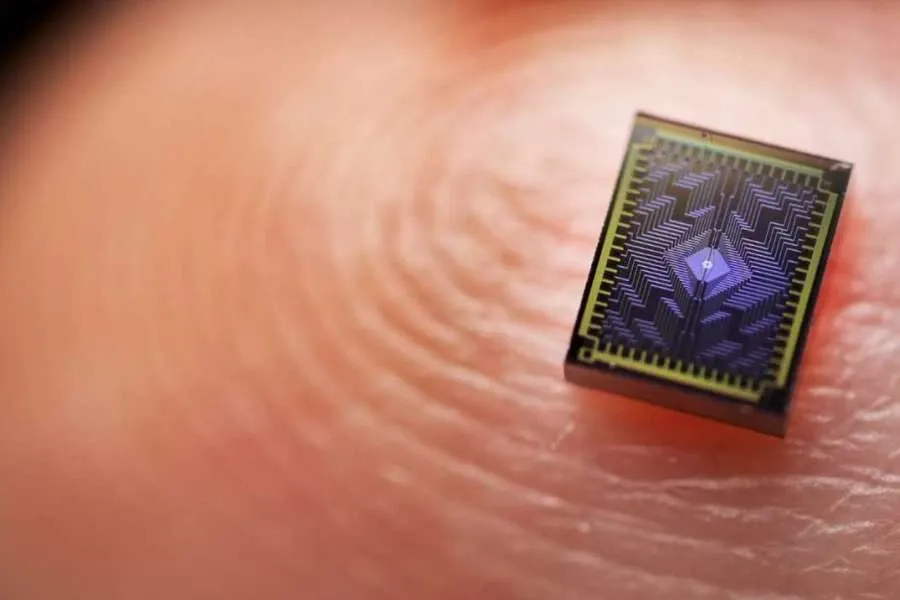
Intel announced the release of its newest quantum research chip, Tunnel Falls, a 12-qubit silicon chip. The company will make it available to the quantum research community. In addition, Intel is collaborating with the Laboratory for Physical Sciences (LPS) at the University of Maryland, College Park’s Qubit Collaboratory (LQC), and a national-level Quantum Information Sciences (QIS) Research Center, to advance quantum-computing research.
“Tunnel Falls is Intel’s most advanced silicon spin qubit chip to date and draws upon the company’s decades of transistor design and manufacturing expertise. The release of the new chip is the next step in Intel’s long-term strategy to build a full-stack commercial quantum computing system. While there are still fundamental questions and challenges that must be solved along the path to a fault-tolerant quantum computer, the academic community can now explore this technology and accelerate research development,“ said Jim Clarke, director of Quantum Hardware at Intel.
The first quantum labs to participate in the program include LPS, Sandia National Laboratories, the University of Rochester, and the University of Wisconsin-Madison. LQC will work alongside Intel to make Tunnel Falls available to additional universities and research labs. The information gathered from these experiments will be shared with the community to advance quantum research and to help Intel improve qubit performance and scalability.
Tunnel Falls is Intel’s first silicon spin qubit device released to the research community. Fabricated on 300-millimeter wafers in the D1 fabrication facility, the 12-qubit device leverages Intel’s most advanced transistor industrial fabrication capabilities, such as extreme ultraviolet lithography (EUV) and gate and contact processing techniques. In silicon spin qubits, information (the 0/1) is encoded in the spin (up/down) of a single electron. Each qubit device is essentially a single electron transistor, which allows Intel to fabricate it using a similar flow to that used in a standard complementary metal oxide semiconductor (CMOS) logic processing line.
Intel believes silicon spin qubits are superior to other qubit technologies because of their synergy with leading-edge transistors. Being the size of a transistor, they are up to 1 million times smaller than other qubit types measuring approximately 50 nanometers by 50 nanometers, potentially allowing for efficient scaling. According to Nature Electronics, silicon may be the platform with the greatest potential to deliver scaled-up quantum computing.
At the same time, utilizing advanced CMOS fabrication lines allows Intel to use innovative process control techniques to enable yield and performance. For example, the Tunnel Falls 12 qubit device has a 95% yield rate across the wafer and voltage uniformity similar to a CMOS logic process, and each wafer provides over 24,000 quantum dot devices. These 12-dot chips can form between four to 12 qubits that can be isolated and used in operations simultaneously depending on how the university or lab operates its systems.

AMD announced that its next-generation EPYC processor, codenamed “Venice,” is the first HPC product in the industry to be taped out and brought up on the TSMC advanced 2nm (N2) process technology.

Optical communications networks are undergoing a transformative phase, driven by the dual demands for increased connectivity and real-time data acquisition.

Researchers at Deutsche Telekom Innovation Laboratories (T-Labs), together with the quantum networking company Qunnect, have reached a milestone on the path to the quantum internet.


