Samsung introduced its newest radio frequency technology based on 8-nanometer process. This foundry technology is expected to provide a ‘one chip solution,’ specifically for 5G communications with support for multi-channel and multi-antenna chip designs.
Samsung’s new process technology is the latest addition to an already broad portfolio of RF-related solutions, including 28nm- and 14nm-based RF. The company has established its RF market leadership through the shipping of more than 500 million mobile RF chips for premium smartphones since 2017.
“Through excellence in innovation and process manufacturing, we’ve reinforced our next-generation wireless communication offerings,“ said Hyung Jin Lee, Master of Foundry Technology Development Team at Samsung. “As 5G mmWave expands, Samsung’s 8nm RF will be a great solution for customers looking for long battery life and excellent signal quality on compact mobile devices.“
With continued scaling to advanced nodes, digital circuits have improved significantly in performance, power consumption, and area, whereas the analog/RF blocks haven’t enjoyed such an improvement due to degenerative parasitics such as increased resistance from narrow line width. As a result, most communications chips tend to see degraded RF characteristics such as deteriorated amplification performance of reception frequency and increased power consumption.
Samsung’s process optimization maximizes channel mobility while minimizing parasitics. Compared to 14nm RF, 8nm RF process technology provides up to a 35 percent increase in power efficiency with a 35 percent decrease in the RF chip area as a result of the RFeFET architectural innovation.
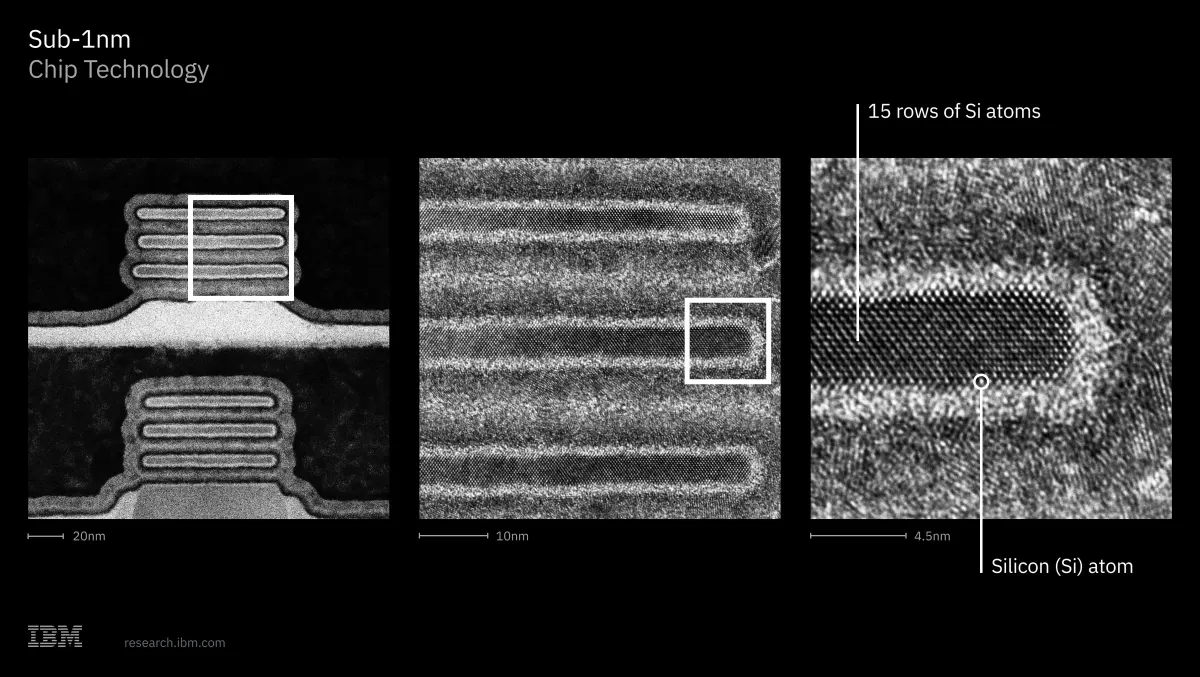
IBM unveiled a major semiconductor breakthrough with the introduction of the world’s first sub-1-nanometer (nm) chip technology, featuring a revolutionary transistor architecture at the 0.7 nm, or 7 angstrom, node.
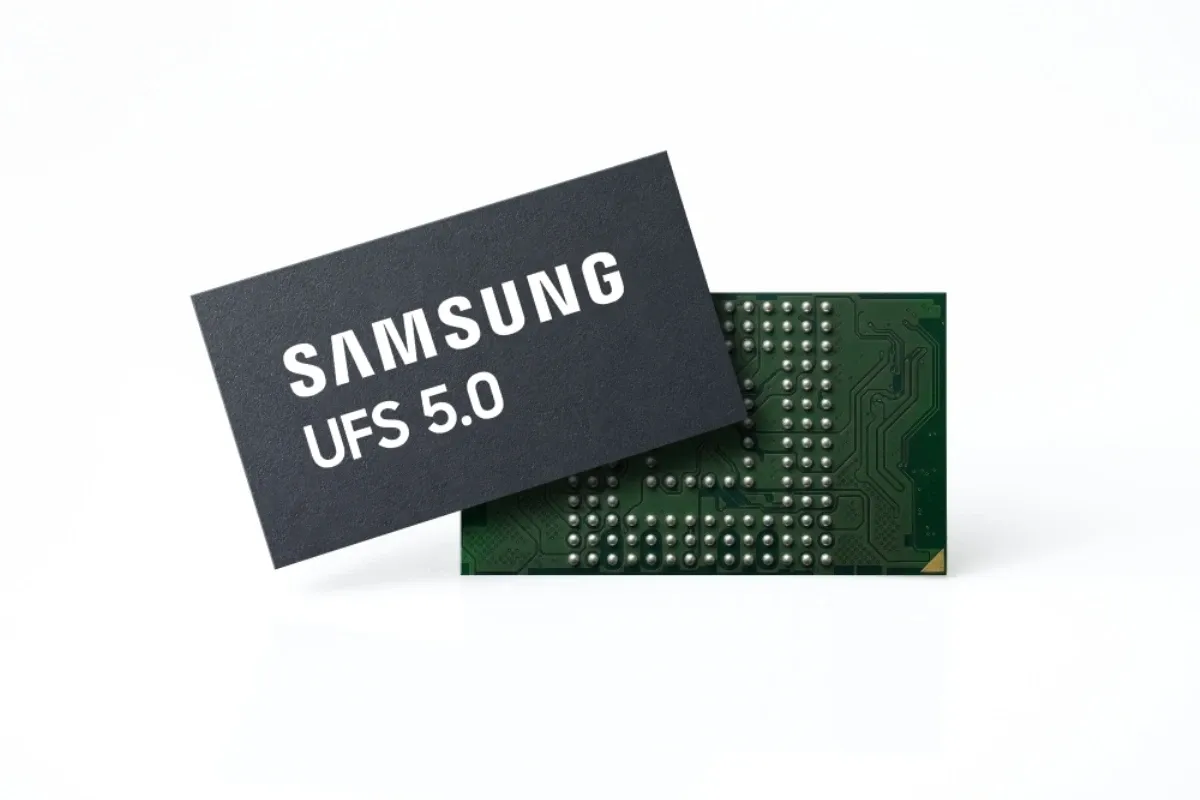
Samsung developed the industry’s fastest Universal Flash Storage (UFS) 5.0 solution, which will help enable seamless and highly efficient AI services on future mobile devices.