Intel Builds the World’s Largest Neuromorphic System
Intel has built the world's largest neuromorphic system code-named Hala Point.

Samsung announced that it has completed all process technology development and has started wafer production of its process node, 7LPP, the 7-nanometer LPP (Low Power Plus) with extreme ultraviolet (EUV) lithography technology. The commercialization of its newest process node, 7LPP gives customers the ability to build a full range of products that will push the boundaries of applications.
“With the introduction of its EUV process node, Samsung has led a quiet revolution in the semiconductor industry,“ said Charlie Bae, executive vice president of foundry sales and marketing team at Samsung. “This fundamental shift in how wafers are manufactured gives our customers the opportunity to significantly improve their products’ time to market with superior throughput, reduced layers, and better yields. We’re confident that 7LPP will be an optimal choice not only for mobile and HPC, but also for a wide range of cutting-edge applications.“
EUV uses 13.5nm wavelength light to expose silicon wafers as opposed to conventional argon fluoride (ArF) immersion technologies that are only able to achieve 193nm wavelengths and require expensive multi-patterning mask sets. EUV enables the use of a single mask to create a silicon wafer layer where ArF can require up to 4 masks to create that same layer. Consequently Samsung’s 7LPP process can reduce the total number of masks by about 20% compared to non-EUV process, enabling customers to save time and cost.
The EUV lithography improvements also deliver increased performance, lower power and smaller area while improving design productivity by reducing mulit-patterning complexity. Compared to its 10nm FinFET predecessors, Samsung’s 7LPP technology not only greatly reduces the process complexity with fewer layers and better yields, but also delivers up to a 40% increase in area efficiency with 20% higher performance or up to 50% lower power consumption.
By 2020, Samsung expects to secure additional capacity with a new EUV line for customers who need high-volume manufacturing for next-generation chip designs. As an EUV pioneer, Samsung has also developed proprietary capabilities such as a unique mask inspection tool that performs early defect detection in EUV masks, allowing those defects to be eliminated early in the manufacturing cycle. The Samsung Advanced Foundry Ecosystem is also fully prepared for the introduction of 7LPP with EUV.
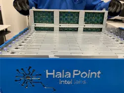
Intel has built the world's largest neuromorphic system code-named Hala Point.

Meta Platforms unveiled the second generation of its Meta Training and Inference Accelerator (MTIA) AI chip.
Intel announced its latest chip to challenge Nvidia’s dominant market position for semiconductors that train and deploy large AI models.


