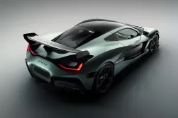
Rimac Nevera R Wins Red Dot Design Award
The Rimac Nevera R, which evolves Nevera from Hyper GT to Hyper Sportscar, has been awarded a coveted Red Dot Award for Product Design 2025.
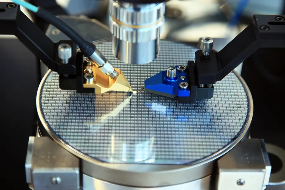
Samsung ordered a new type of advanced chipmaking machinery. The company targets increased production yield of its high bandwidth memory (HBM) chips to win business from Nvidia.
The South Korean chipmaker will deploy the mass reflow molded underfill (MR-MUF) technique, first used by rival SK Hynix, to boost its HBM chip yields. Mass production using the new method won’t start until next year at the earliest as tests are carried out.
Samsung denied it is switching technologies, claiming the current non-conductive film (NCF) method was the optimal solution and will be used to make new HBM chips. But according to sources, Samsung will use both techniques for future high-end chips, noting the yield for its latest HBM chip using NCF is 10% to 20%, compared with 60% to 70% for SK Hynix.
Samsung is reportedly discussing sourcing MUF materials from various suppliers, including Japan-based Nagase. The vendor recently said it started sampling its latest HBM chip, the HBM3E, to customers, with mass production expected in the first half of this year.
The Rimac Nevera R, which evolves Nevera from Hyper GT to Hyper Sportscar, has been awarded a coveted Red Dot Award for Product Design 2025.

Social media company X's CEO, Linda Yaccarino, is leaving her position.
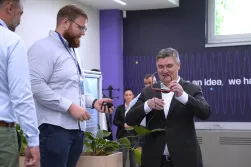
Ericsson Nikola Tesla organized a new edition of its Technology Days Conference.


