Samsung Begins Shipment of Its Latest HBM Chip Samples
Samsung announced that it has begun shipping the industry’s first 12-layer HBM4E samples to major global customers.
IBM and Samsung announced a breakthrough in semiconductor design utilizing a new vertical transistor architecture that demonstrates a path to scaling beyond nanosheet and has the potential to reduce energy usage by 85 percent compared to a scaled fin field-effect transistor (finFET). The global semiconductor shortage has highlighted the critical role of investment in chip research and development and the importance of chips in everything from computing, to appliances, to communication devices, transportation systems, and critical infrastructure.
This collaborative approach to innovation makes the Albany Nanotech Complex a world-leading ecosystem for semiconductor research and creates a strong innovation pipeline, helping to address manufacturing demands and accelerate the growth of the global chip industry. The new vertical transistor breakthrough could help the semiconductor industry continue its relentless journey to deliver significant improvements, including potential device architecture that enables semiconductor device scaling to continue beyond nanosheet; cell phone batteries that could go over a week without being charged, instead of days; energy-intensive processes, such as crypto mining operations and data encryption, could require significantly less energy and have a smaller carbon footprint, and continued expansion of the Internet of Things (IoT) and edge devices with lower energy needs, allowing them to operate in more diverse environments like ocean buoys, autonomous vehicles, and spacecraft.
"Today's technology announcement is about challenging convention and rethinking how we continue to advance society and deliver innovations that improve life, business and reduce our environmental impact," said Mukesh Khare, Vice President of Hybrid Cloud and Systems at IBM Research. "Given the constraints, the industry is currently facing along multiple fronts, IBM and Samsung are demonstrating our commitment to joint innovation in semiconductor design and a shared pursuit of what we call 'hard tech.'
Moore's Law, the principle that the number of transistors incorporated in a densely populated IC chip will approximately double every two years, is quickly nearing what is considered insurmountable barriers. Simply put, as more and more transistors are crammed into a finite area, engineers are running out of space. Historically, transistors have been built to lie flat upon the surface of a semiconductor, with the electric current flowing laterally, or side-to-side, through them. With new Vertical Transport Field-Effect Transistors or VTFET, IBM and Samsung have successfully implemented transistors that are built perpendicular to the surface of the chip with a vertical, or up-and-down, current flow.
The VTFET process addresses many barriers to performance and limitations to extend Moore's Law as chip designers attempt to pack more transistors into a fixed space. It also influences the contact points for the transistors, allowing for greater current flow with less wasted energy. Overall, the new design aims to deliver a two times improvement in performance or an 85 percent reduction in energy use as compared to scaled finFET alternatives.
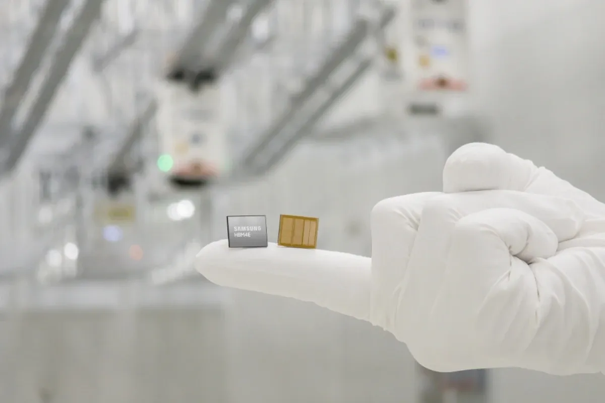
Samsung announced that it has begun shipping the industry’s first 12-layer HBM4E samples to major global customers.
In recent years, Moore's Law, which has guided the semiconductor industry for more than five decades, has faced severe physical limits and diminishing economic returns.
IBM and the US Department of Commerce (DoC) announced a Letter of Intent to build an American quantum chip foundry.