Samsung Begins Shipment of Its Latest HBM Chip Samples
Samsung announced that it has begun shipping the industry’s first 12-layer HBM4E samples to major global customers.

Samsung updated its semiconductor process roadmap at its foundry forum in San Jose. The company targets mass production of a fourth-generation 2nm chip in 2027 and an upgraded 4nm silicon in 2025.
At the Samsung Foundry Forum 2024, the company stated its latest 2nm process uses advanced backside power delivery network technology to improve power efficiency and lower temperatures. The SF2Z process node will be ready for mass production in 2027. The new SF4U process, referred to as a high-value 4nm variant, offers power, performance, and area improvements using optical shrink, with mass production scheduled for 2025, the company said.
Choi Si-young, president of the company’s foundry business, stated high-performance, low-power semiconductors are key at a time when numerous technologies are evolving around AI. He noted Samsung plans to introduce integrated, co-packaged optics technology for high-speed, low-power data processing. The company also claimed its gate-all-around (GAA) transistor architecture is maturing in performance and yield.
Samsung noted preparations for the 1.4nm process (SF1.4) are progressing smoothly, with performance and yield targets on track, adding it is actively shaping future process technologies below 1.4nm through material and structural innovations. Its first-generation 2nm process, SF2, will begin in 2025, with an upgraded SF2P version to be ready in 2026.
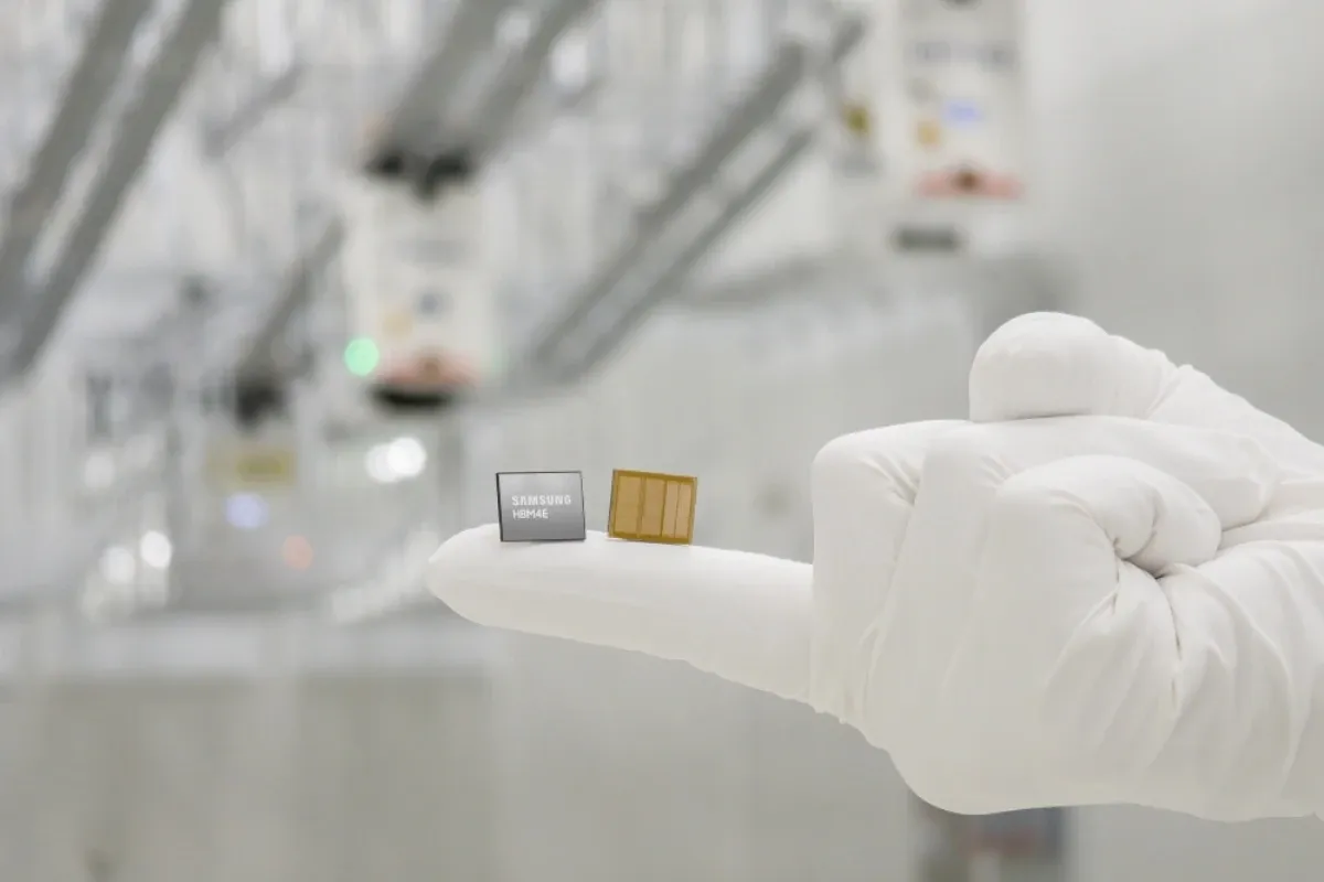
Samsung announced that it has begun shipping the industry’s first 12-layer HBM4E samples to major global customers.

In recent years, Moore's Law, which has guided the semiconductor industry for more than five decades, has faced severe physical limits and diminishing economic returns.

IBM and the US Department of Commerce (DoC) announced a Letter of Intent to build an American quantum chip foundry.