Qualcomm Announces Snapdragon 8 Gen 5 Platform
Qualcomm added its latest smartphone platform to its premium-tier Snapdragon range.
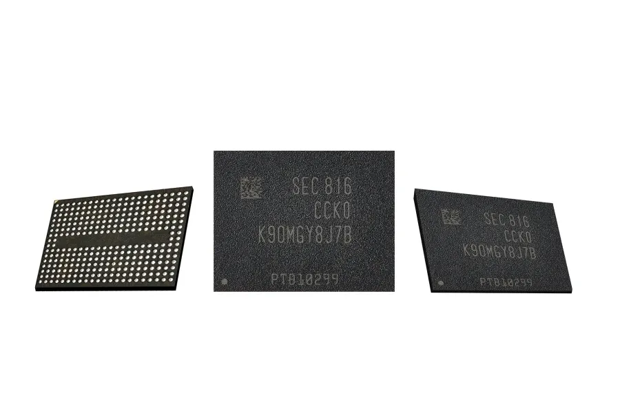
Samsung announced that it has begun mass producing its fifth-generation V-NAND memory chips with the fastest data transfers now available.
In the industry’s first use of the ‘Toggle DDR 4.0’ interface, the speed for transmitting data between storage and memory over Samsung’s new 256-gigabit (Gb) V-NAND has reached 1.4-gigabits per second (Gbps), a 40-percent increase from its 64-layer predecessor.
The energy efficiency of new V-NAND remains comparable to that of the 64-layer chip, primarily because the operating voltage has been reduced from 1.8 volts to 1.2 volts. The new V-NAND also has the fastest data write speed to date at 500-microseconds (μs), which represents about a 30-percent improvement over the write speed of the previous generation, while the response time to read-signals has been reduced to 50μs.
Packed inside fifth-generation V-NAND are more than 90 layers of ‘3D charge trap flash (CTF) cells,’ the largest amount in the industry, stacked in a pyramid structure with microscopic channel holes vertically drilled throughout. These channel holes, which are only a few hundred-nanometers wide, contain more than 85 billion CTF cells that can store three bits of data each.
Thanks to enhancements in the V-NAND’s atomic layer deposition process, manufacturing productivity has also increased by more than 30 percent. The technique allows the height of each cell layer to be reduced by 20 percent, prevents crosstalk between cells and increases the efficiency of the chip’s data processing. Samsung will be quickly ramping up production of its fifth-generation V-NAND to meet a wide range of market needs.

Qualcomm added its latest smartphone platform to its premium-tier Snapdragon range.

Cisco and IBM set a target for a proof-of-concept of large-scale networking technology for quantum computing.

According to information available today, November 18, 2025, Cloudflare, a vital provider of Internet infrastructure and security, experienced a massive global service outage that resulted in widespread failure to access countless online services. The incident began around 11:20 GMT (12:20 CET), causing a global wave of disruption that affected key digital platforms across North America, Europe, and Asia.


