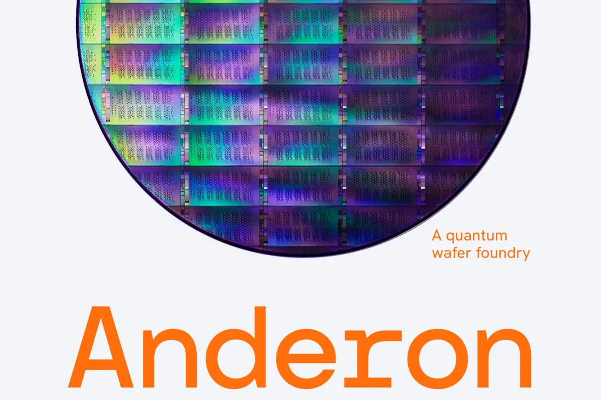
IBM Announces First Purpose-Built Quantum Foundry
IBM and the US Department of Commerce (DoC) announced a Letter of Intent to build an American quantum chip foundry.
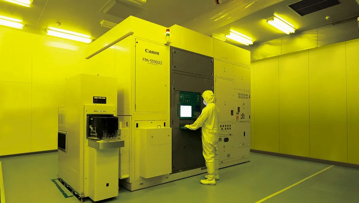
Canon unveiled a new line of advanced chipmaking equipment featuring nanoimprint lithography (NIL) technology. The company claims that the new process is simpler than extreme ultraviolet lithography (EUV) and can significantly reduce power consumption and costs.
The company explained the technology in a statement saying it executes circuit pattern transfer and enables patterns with a minimum linewidth of 14nm, equivalent to the 5nm-node required to produce the most advanced semiconductors available. Canon noted that, with further improvement, NIL is expected to enable circuit patterning with a minimum linewidth of 10nm, which corresponds to next-generation 2nm-node production.
With nanoimprint lithography, Canon noted fine circuit patterns can be accurately reproduced on a wafer, allowing complex 2D or 3D circuit patterns to be formed in a single imprint, which may reduce the cost of ownership. Since the product does not require a light source with a special wavelength for fine circuits, it can reduce power consumption significantly compared with photolithography equipment, Canon stated.
IBM and the US Department of Commerce (DoC) announced a Letter of Intent to build an American quantum chip foundry.

Samsung and Google unveiled a pair of smart glasses designs set to be released in selected markets later this year.
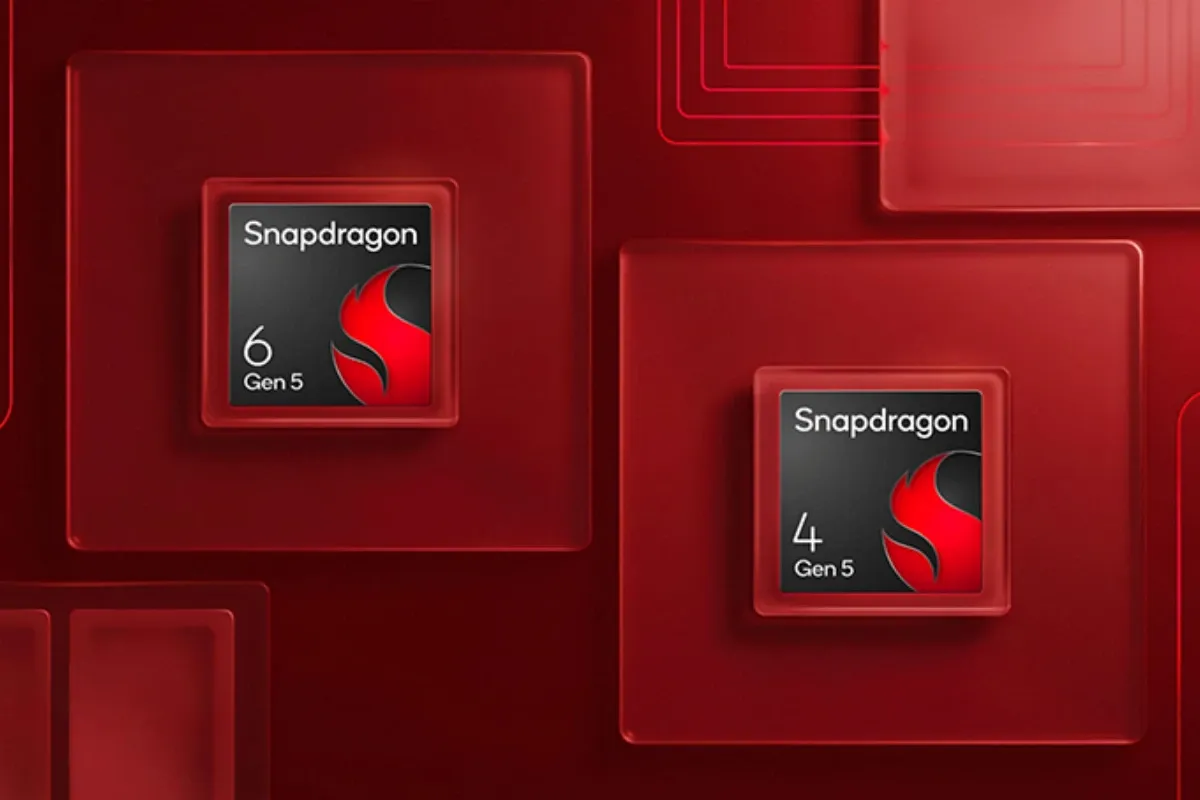
Qualcomm unveiled two new mobile chips aiming to bring advanced smartphone capabilities to a wider audience.